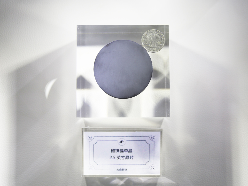
Application areas:
It is also widely used as infrared detectors HgCdTe epitaxial substrate and nuclear radiation detector, it has excellent optical and electrical properties, can be at room temperature directly to X ray and turn into electron photon, is by far the room temperature X ray and gamma ray detector is the most ideal semiconductor material. Compared with the silicon and germanium geophone, the CdZnTe crystal is the only semiconductor that works at room temperature and can handle two million photons / (s. Mm). In addition, the CdZnTe crystal is better than all the optical splitters that can be bought. CdZnTe detector has many advantages, making it more and more widely used, nuclear safety, environmental monitoring, astrophysics and other fields have been applied. In the field of scientific research, the CdZnTe detector has a great potential in high energy physics, for example, it can be used in the acceleration system of high energy particles. Compound semiconductor detectors are very competitive, and it is expected that the application of particle physics will be greatly developed. In addition, the CdZnTe detector has a broad application prospect in the field of astronomical and physical research. At present, the research of CdZnTe detector is a very meaningful new topic in a rapid development stage.
Development direction:
At present, the two important development directions of CdZnTe detector are: multi block large volume parallel detector and surface element array detector. The former is composed of a plurality of CdZnTe crystal array size greater than 1cm, this type of detector solves the single detector has the advantages of small volume, low efficiency of the total detection, greatly shorten the measurement time, especially suitable for portable spectrometer system, radiation monitoring can be applied to the environment, port and railway cargo etc.. The latter is composed of CdZnTe crystal surface element array, which is mainly used in nuclear medicine, astrophysics and other fields of energy spectrum imaging.
The development and use of the CdZnTe detector, the detector to obtain high performance high photon as possible, with high-quality CdZnTe semiconductor crystal preparation technology continues to improve, the carrier collection process of the rapid development of microelectronics and further understanding of low noise, CdZnTe detectors will be applied in more extensive field.